- 您现在的位置:买卖IC网 > Sheet目录3887 > PIC16F872T-E/SO (Microchip Technology)IC MCU CMOS 20MHZ 2K FLSH 28SOIC
124
8048C–AVR–02/12
ATtiny43U
ADC conversion completes. The CPU will remain in active mode until a new sleep command
is executed.
Note that the ADC will not automatically be turned off when entering other sleep modes than Idle
mode and ADC Noise Reduction mode. The user is advised to write zero to ADEN before enter-
ing such sleep modes to avoid excessive power consumption.
16.8
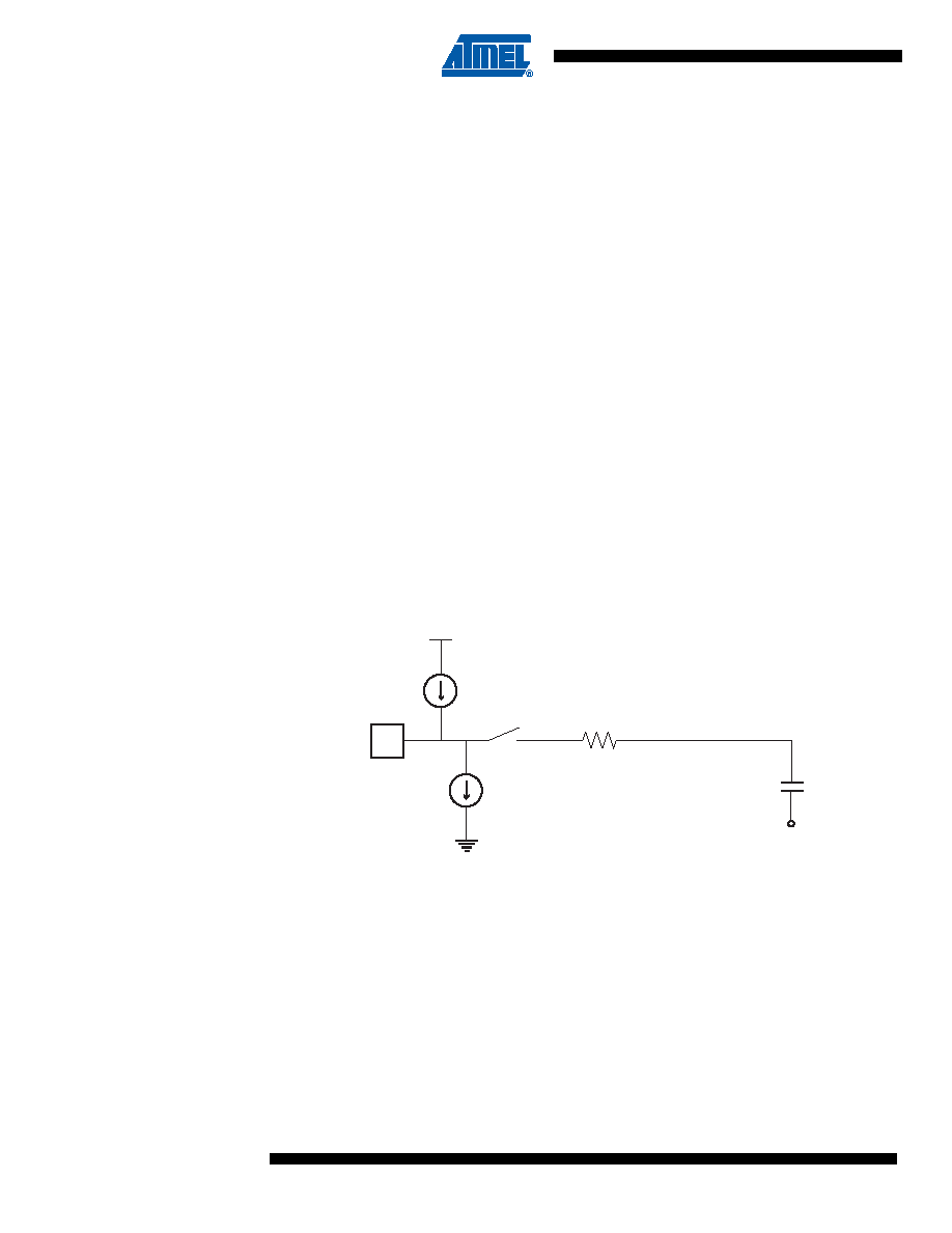
Analog Input Circuitry
The analog input circuitry for single ended channels is illustrated in Figure 16-8. An analog
source applied to ADCn is subjected to the pin capacitance and input leakage of that pin, regard-
less of whether that channel is selected as input for the ADC. When the channel is selected, the
source must drive the S/H capacitor through the series resistance (combined resistance in the
input path).
The ADC is optimized for analog signals with an output impedance of approximately 10k
Ω or
less. If such a source is used, the sampling time will be negligible. If a source with higher imped-
ance is used, the sampling time will depend on how long time the source needs to charge the
S/H capacitor, which can vary widely. The user is recommended to only use low impedance
sources with slowly varying signals, since this minimizes the required charge transfer to the S/H
capacitor.
In order to avoid distortion from unpredictable signal convolution, signal components higher than
the Nyquist frequency (f
ADC/2) should not be present. The user is advised to remove high fre-
quency components with a low-pass filter before applying the signals as inputs to the ADC.
Figure 16-8. Analog Input Circuitry
Note:
The capacitor in the figure depicts the total capacitance, including the sample/hold capacitor and
any stray or parasitic capacitance inside the device. The value given is worst case.
16.9
Analog Noise Canceling Techniques
Digital circuitry inside and outside the device generates EMI which might affect the accuracy of
analog measurements. If conversion accuracy is critical, the noise level can be reduced by
applying the following techniques:
Keep analog signal paths as short as possible.
Make sure analog tracks run over the analog ground plane.
ADCn
IIH
1..100 k
ohm
CS/H= 14 pF
VCC/2
IIL
发布紧急采购,3分钟左右您将得到回复。
相关PDF资料
PIC16F727-E/P
IC PIC MCU FLASH 8KX14 40-DIP
PIC16F871T-E/PT
IC MCU CMOS 20MHZ 2K FLSH 44TQFP
PIC16F871T-E/L
IC MCU CMOS 20MHZ 2K FLSH 44PLCC
PIC16F871-E/PT
IC MCU CMOS 20MHZ 2K FLSH 44TQFP
PIC16F871-E/L
IC MCU CMOS 20MHZ 2K FLSH 44PLCC
PIC16F870T-E/SS
IC MCU CMOS 20MHZ 2K FLSH 28SSOP
PIC16F870T-E/SO
IC MCU CMOS 20MHZ 2K FLSH 28SOIC
PIC16F84AT-20E/SS
IC MCU CMOS 20MHZ 1K FLSH 20SSOP
相关代理商/技术参数
PIC16F872T-E/SS
功能描述:8位微控制器 -MCU 3.5KB 128 RAM 22 I/O RoHS:否 制造商:Silicon Labs 核心:8051 处理器系列:C8051F39x 数据总线宽度:8 bit 最大时钟频率:50 MHz 程序存储器大小:16 KB 数据 RAM 大小:1 KB 片上 ADC:Yes 工作电源电压:1.8 V to 3.6 V 工作温度范围:- 40 C to + 105 C 封装 / 箱体:QFN-20 安装风格:SMD/SMT
PIC16F872T-I/SO
功能描述:8位微控制器 -MCU 3.5KB 128 RAM 22 I/O RoHS:否 制造商:Silicon Labs 核心:8051 处理器系列:C8051F39x 数据总线宽度:8 bit 最大时钟频率:50 MHz 程序存储器大小:16 KB 数据 RAM 大小:1 KB 片上 ADC:Yes 工作电源电压:1.8 V to 3.6 V 工作温度范围:- 40 C to + 105 C 封装 / 箱体:QFN-20 安装风格:SMD/SMT
PIC16F872T-I/SS
功能描述:8位微控制器 -MCU 3.5KB 128 RAM 22 I/O RoHS:否 制造商:Silicon Labs 核心:8051 处理器系列:C8051F39x 数据总线宽度:8 bit 最大时钟频率:50 MHz 程序存储器大小:16 KB 数据 RAM 大小:1 KB 片上 ADC:Yes 工作电源电压:1.8 V to 3.6 V 工作温度范围:- 40 C to + 105 C 封装 / 箱体:QFN-20 安装风格:SMD/SMT
PIC16F872T-I/SS033
制造商:Microchip Technology Inc 功能描述:
PIC16F873-04/SO
功能描述:8位微控制器 -MCU 7KB 192 RAM 22 I/O RoHS:否 制造商:Silicon Labs 核心:8051 处理器系列:C8051F39x 数据总线宽度:8 bit 最大时钟频率:50 MHz 程序存储器大小:16 KB 数据 RAM 大小:1 KB 片上 ADC:Yes 工作电源电压:1.8 V to 3.6 V 工作温度范围:- 40 C to + 105 C 封装 / 箱体:QFN-20 安装风格:SMD/SMT
PIC16F873-04/SO
制造商:Microchip Technology Inc 功能描述:8BIT FLASH MCU SMD 16F873 SOIC28
PIC16F873-04/SP
功能描述:8位微控制器 -MCU 7KB 192 RAM 22 I/O RoHS:否 制造商:Silicon Labs 核心:8051 处理器系列:C8051F39x 数据总线宽度:8 bit 最大时钟频率:50 MHz 程序存储器大小:16 KB 数据 RAM 大小:1 KB 片上 ADC:Yes 工作电源电压:1.8 V to 3.6 V 工作温度范围:- 40 C to + 105 C 封装 / 箱体:QFN-20 安装风格:SMD/SMT
PIC16F873-04/SP
制造商:Microchip Technology Inc 功能描述:IC 8BIT FLASH MCU 16F873 SDIL28